Lab 2: Multiplexed 7-Segment Display
Introduction
In this lab, a design was implemented on the UPduino v3.1 FPGA to time-multiplex a dual seven-segment display. The design used a single set of GPIO pins and a single seven-segment HDL module, switching between the two digits at a rate high enough that the multiplexing was not perceptible to the human eye.
Design and Testing Methodology
The iCE40 UltraPlus HSOSC primitive generated the main clock, which was divided down to 60 Hz as the base refresh frequency for the display. At this rate, the human eye can no longer perceive individual refresh events, and bleeding between digits is minimized.
An 8-position DIP switch controlled the HDSP-521A dual seven-segment display. The lower four switches set the value for the first digit. The upper four switches set the value for the second digit.
When the internal multiplexing clock was low, the first four switch inputs were selected and the first digit’s anode was driven. When the clock was high, the second set of four switches was selected and the second digit’s anode was driven.
The sum of the two hex values displayed on the HDSP-521A was shown in binary on the on-board LEDs of the E155 Development Board. These LEDs were placed in series with 1 kΩ resistors to limit current.
The Seven Segment Display module- a priority encoder- converted the 4-bit switch inputs into the corresponding seven-segment code. The HDSP-521A required more current than the FPGA could supply directly, so two 2N3906 PNP transistors were used to drive the common anodes. Each segment cathode was connected through a 330 Ω current-limiting resistor to achieve approximately 3 mA of segment current over the effective voltage drop:
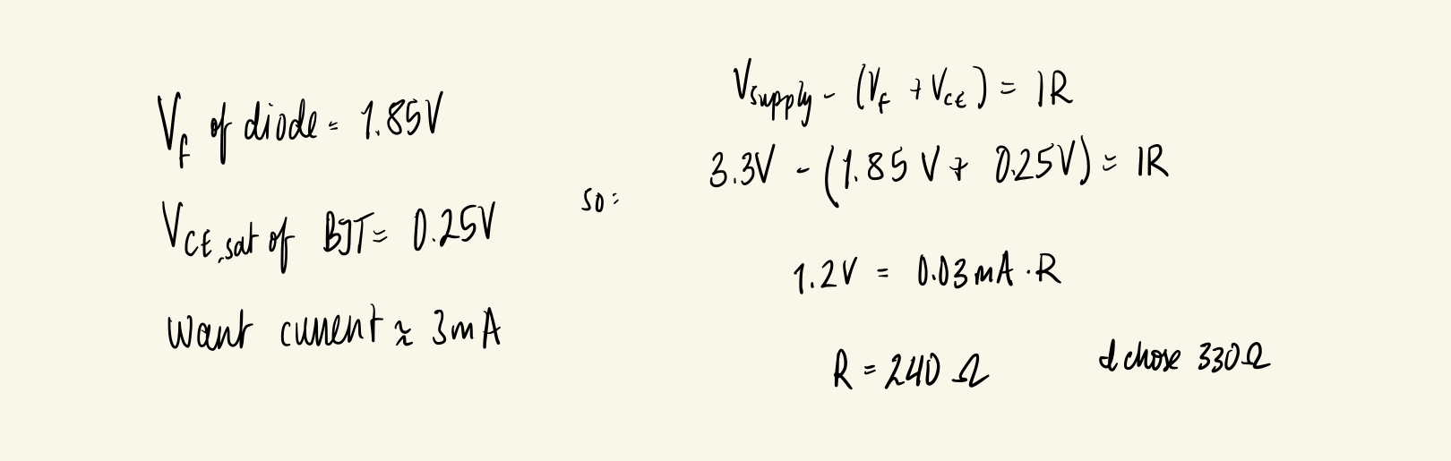
A 460 Ω resistor was placed between each transistor base and its corresponding GPIO pin to keep the base current below 5 mA, as specified in the datasheet. The calculation for this value is shown in Figure 1.
![]()
To control the input to the Seven Segment Display, a priority encoder was used. The output signals were mapped to their respective pins on the input of the HDSP-511A Seven Segment Display.
Block Diagram
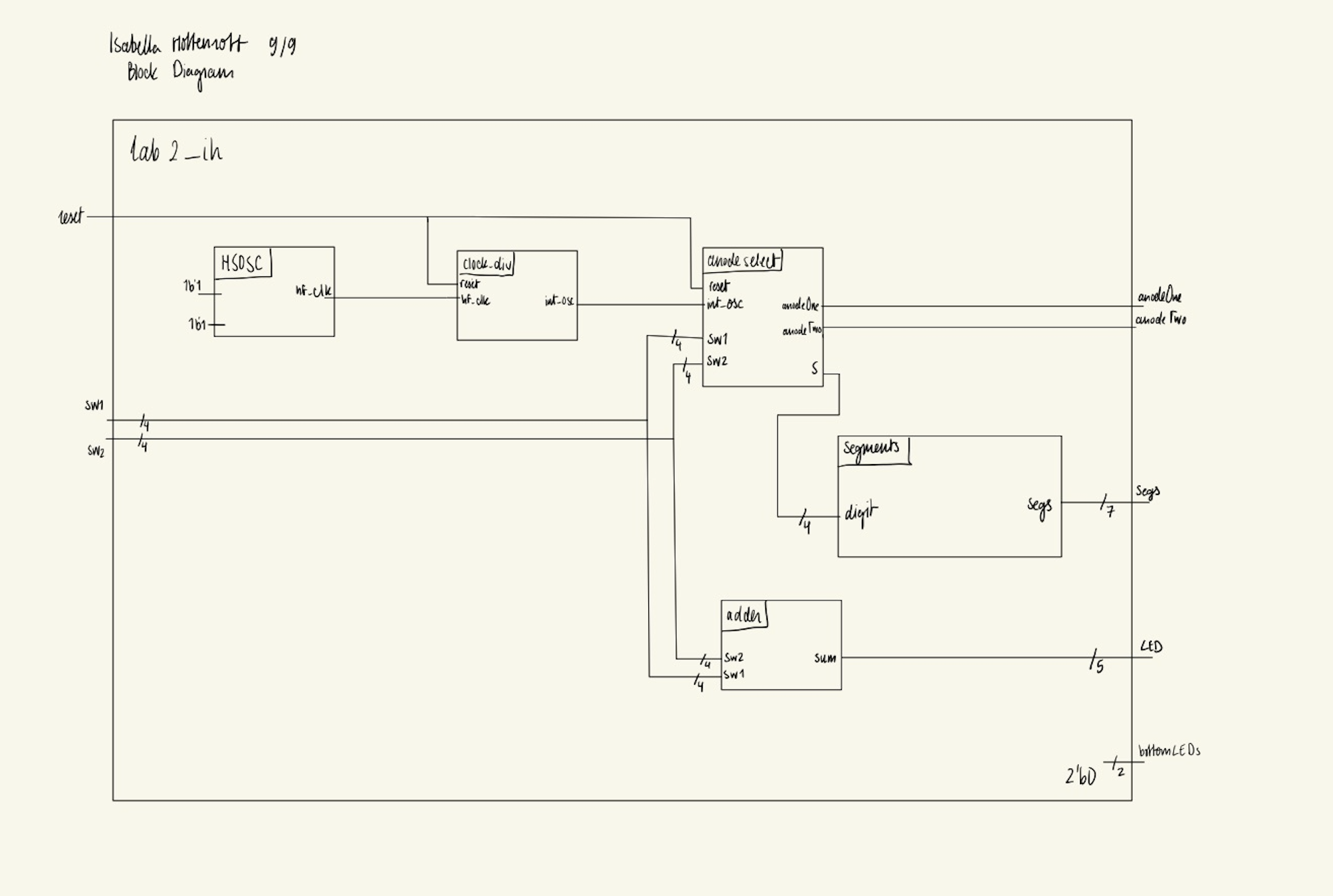
The block diagram above illustrates the lab2_ih design. The top level module, lab2_ih, takes in inputs: reset, sw1, and sw2. The module outputs to outputs to five leds (led), a single set of GPIO pins for the dual seven segment (segs), to both transistors to illuminate the proper segment anode (anodeOne, anodeTwo), and to the two remaining on-board LEDs to keep them from floating (bottomLEDs). Lab2_ih instantiates five submodules: the high-speed oscillator block (hf_osc), the clock divider to 60 Hz (clock_div), the adder (adder), the seven segments priority encoder (segments), and the anode-selecting module (anodeselect).
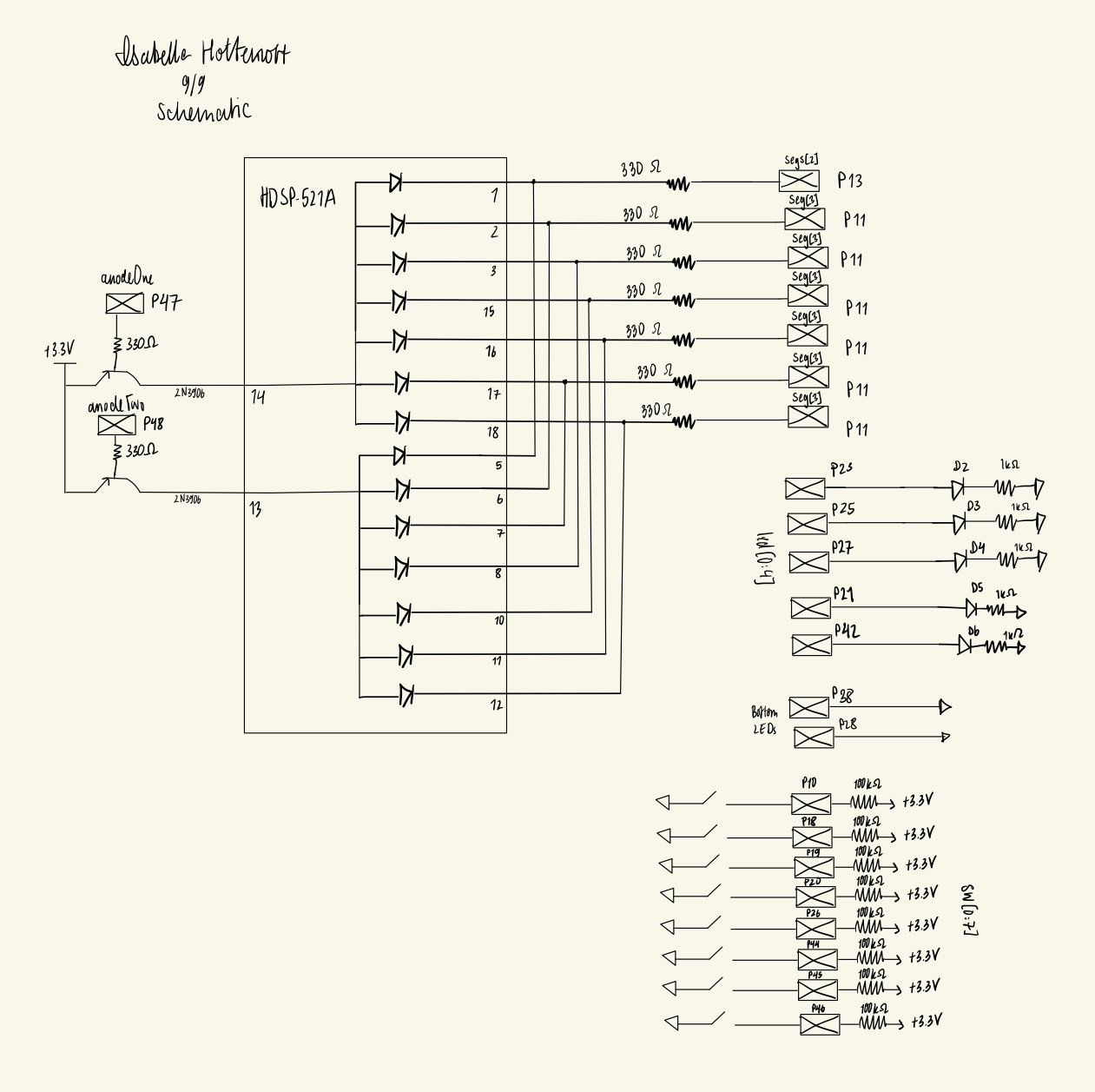
Schematic
The schematic shows the physical layout of the breadboard. Corresponding segment cathodes from the two digits of the dual display are tied together (e.g., segment A of digit 1 shares a node with segment A of digit 2). Each shared node is connected through a 330 Ω current-limiting resistor to a GPIO pin.
The on-board LEDs use 1 kΩ series resistors for current limiting. For each PNP transistor, the emitter is connected to 3.3 V, the collector is connected to the common anode of one digit, and the base is driven through a 460 Ω resistor from the FPGA output. This keeps the base current below 5 mA and within the FPGA’s current specifications.
Results and Discussion
The design met all intended objectives. The DIP switches correctly drove the two hex digits, the binary sum displayed on the on-board LEDs matched the expected values, and the dual seven-segment display showed two stable, distinct hex values with no discernible flicker or bleeding.
Testbench Simulation
A testbench simulation was produced for every module in the design.
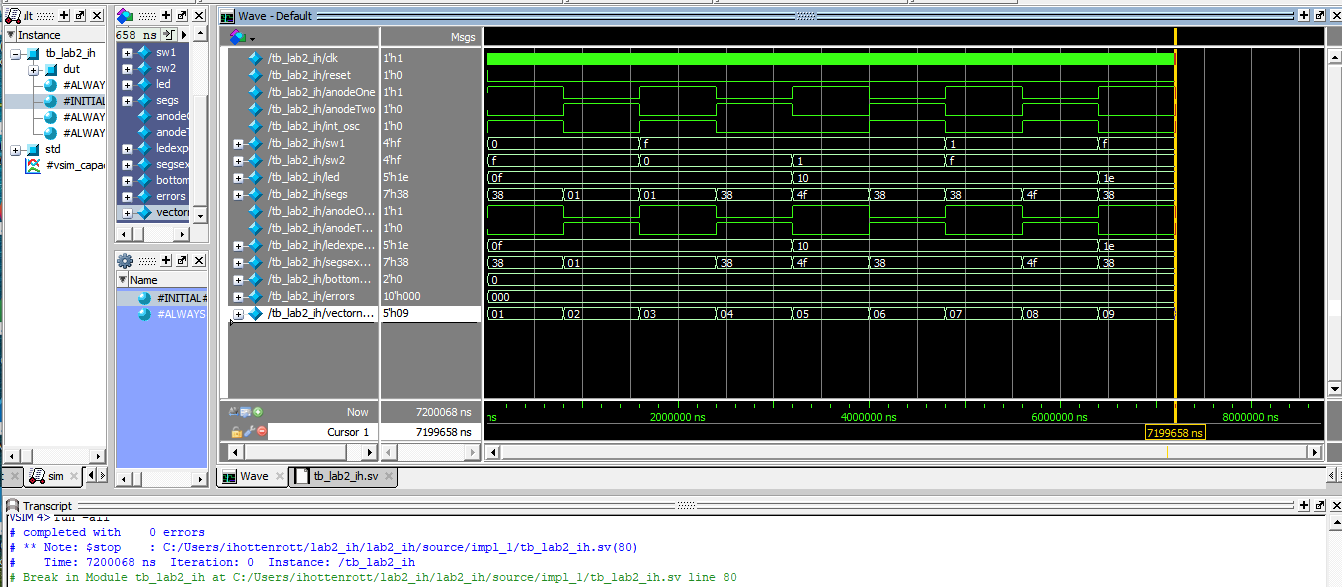
tb_lab2_ih:
The testbench for lab2_ih can be found here. For this simulation, the high-speed oscillator primitive was commented out and replaced with a test clock. Ten known input cases were applied and the outputs were compared against expected values. No mismatches were observed.
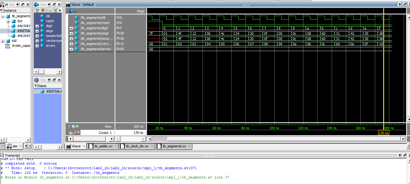
tb_segments:
The testbench for the segments module can be found here. All possible 4-bit input combinations were exercised, and the resulting seven-segment outputs were verified to match the expected patterns. No errors occurred.
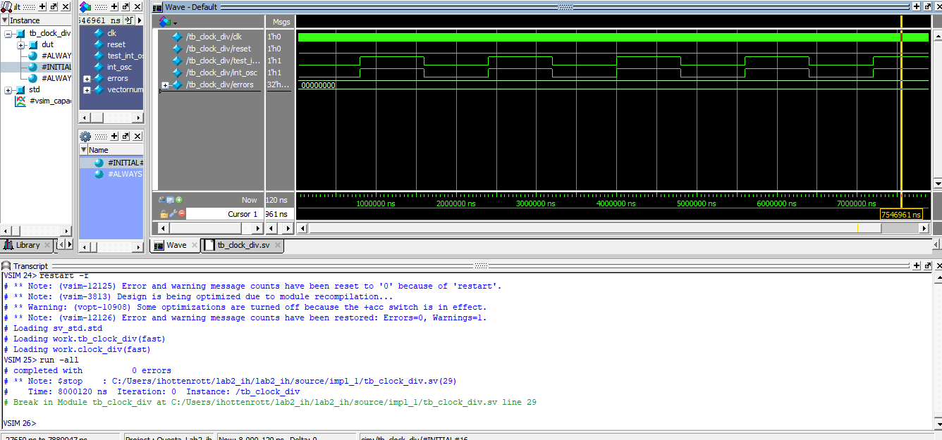
tb_clock_div:
The testbench for the clock divider module can be found here. A test oscillator was created that toggled every 800,000 time steps (with two time steps representing one full clock cycle). The divider’s output was compared against this reference. The HSOSC provides a 48 MHz clock, and the divider reduces it by a factor of 800,000 to 60 Hz. The simulated divided clock matched the reference, confirming correct frequency division. No errors occurred.
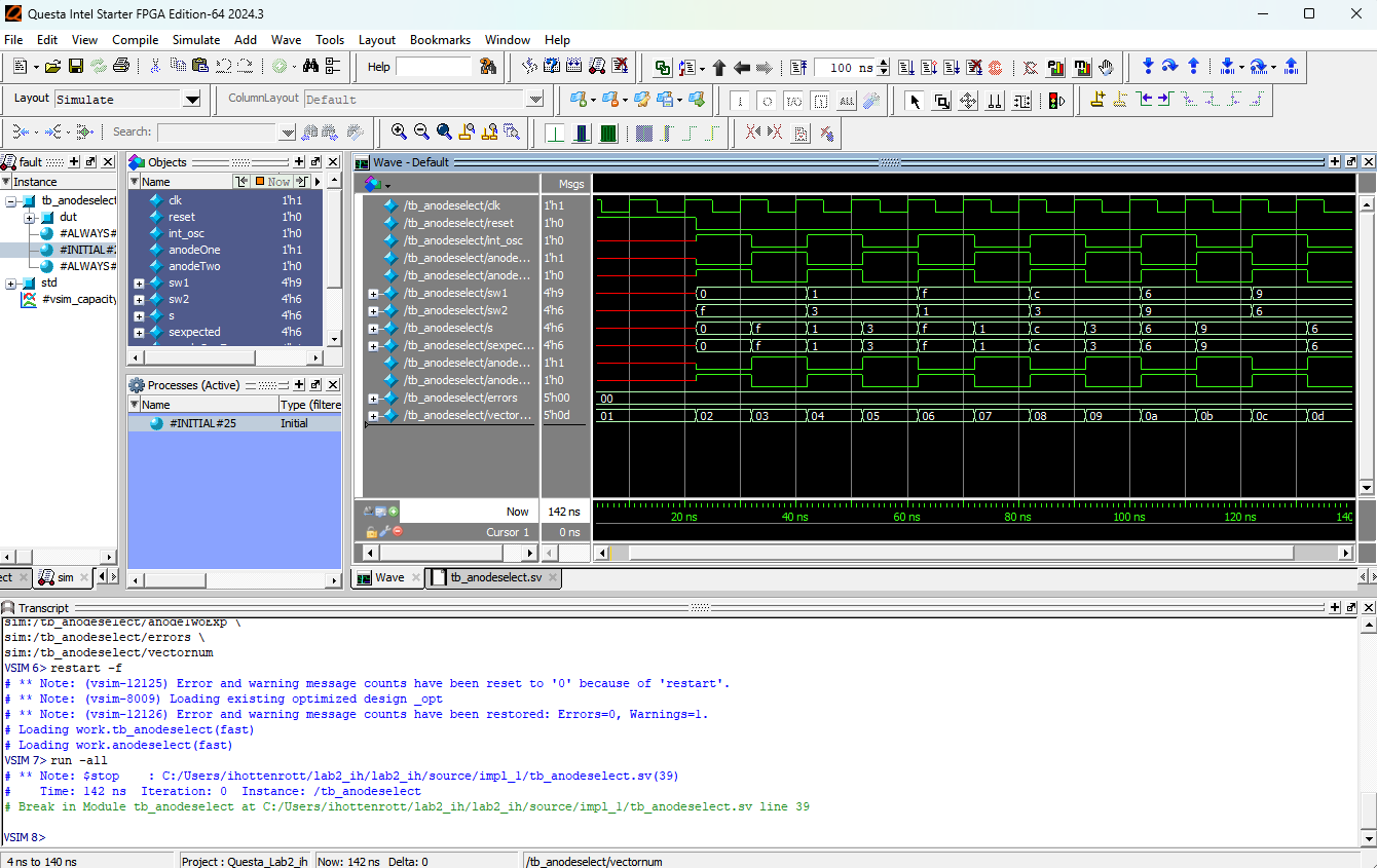
tb_anodeselect:
The testbench for the anodeselect module can be found here. Twelve handwritten test vectors were applied to verify that the 4-bit input produces the correct output from the segments module at each phase of the multiplexing clock, and that only one anode is ever asserted high. All checks passed with no errors.
tb_adder:
The testbench for the adder module can be found here. A SystemVerilog function iterated through all possible input combinations to verify the correctness of the sum. All additions produced the expected binary output, and no errors occurred.

Conclusion
This design successfully drove a dual seven-segment display using a single seven-segment decoder through time-multiplexing. The BJT ensured that sufficient, but not excessive, current flowed through each segment in accordance with the component datasheets. The design functioned correctly in both hardware and simulation, and met all specified objectives.
AI Prototype Summary
The prompt that I provided the LLM was: “Write SystemVerilog HDL to time multiplex a single seven segment decoder (that decodes from four bits to a common anode seven segment display) to decode two sets of input bits and drive two sets of seven output bits.”
The LLM’s response, as well as my evaluation of the response, can be found here