Lab 1: FPGA and MCU Setup and Testing
Introduction
This lab implemented a simple design on the UPduino v3.1 FPGA to validate proper assembly and functionality of the E155 Development Board. This lab demonstrated correct operation of the development board’s LEDs, the FPGA’s on-board high-speed oscillator, and a seven-segment display.
Design and Testing Methodology
The iCE40 UltraPlus HSOSC primitive was used to generate a clock signal at 48 MHz. A separate clock divider module was created to divide the HSOSC signal to a frequency of 2.4 Hz using a counter that reset every 10,000 counts, and providing a slow blink signal for an external LED.
Control logic for the remaining on-board LEDs consisted of simple combinational operations (XOR and AND) driven by the switch inputs.
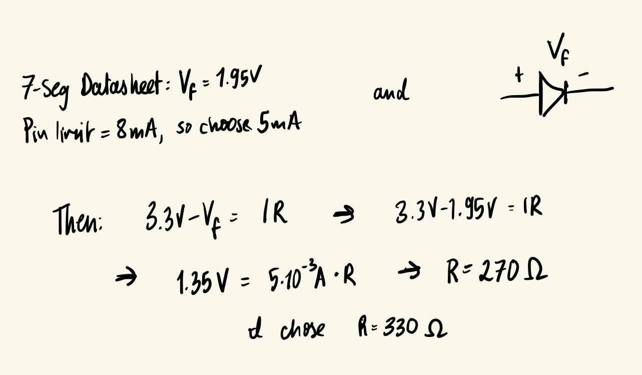
A priority encoder was used to select which segment of the seven-segment display would illuminate. Its outputs were mapped to the pins of an HDSP-511A common-anode display. Each segment was activated by grounding its corresponding GPIO pin, producing the required 3.3 V drop across the diode. With a forward voltage of 1.95 V and a desired diode current of around 5 mA, 330 Ω series resistors were selected as current-limiting elements. The corresponding calculations are shown in Figure 1.
To deactivate a segment, the GPIO pin was driven high to eliminate voltage drop and prevent current flow.
Technical Documentation
The source code for Lab 1 can be found in the following GitHub repository.
Block Diagram
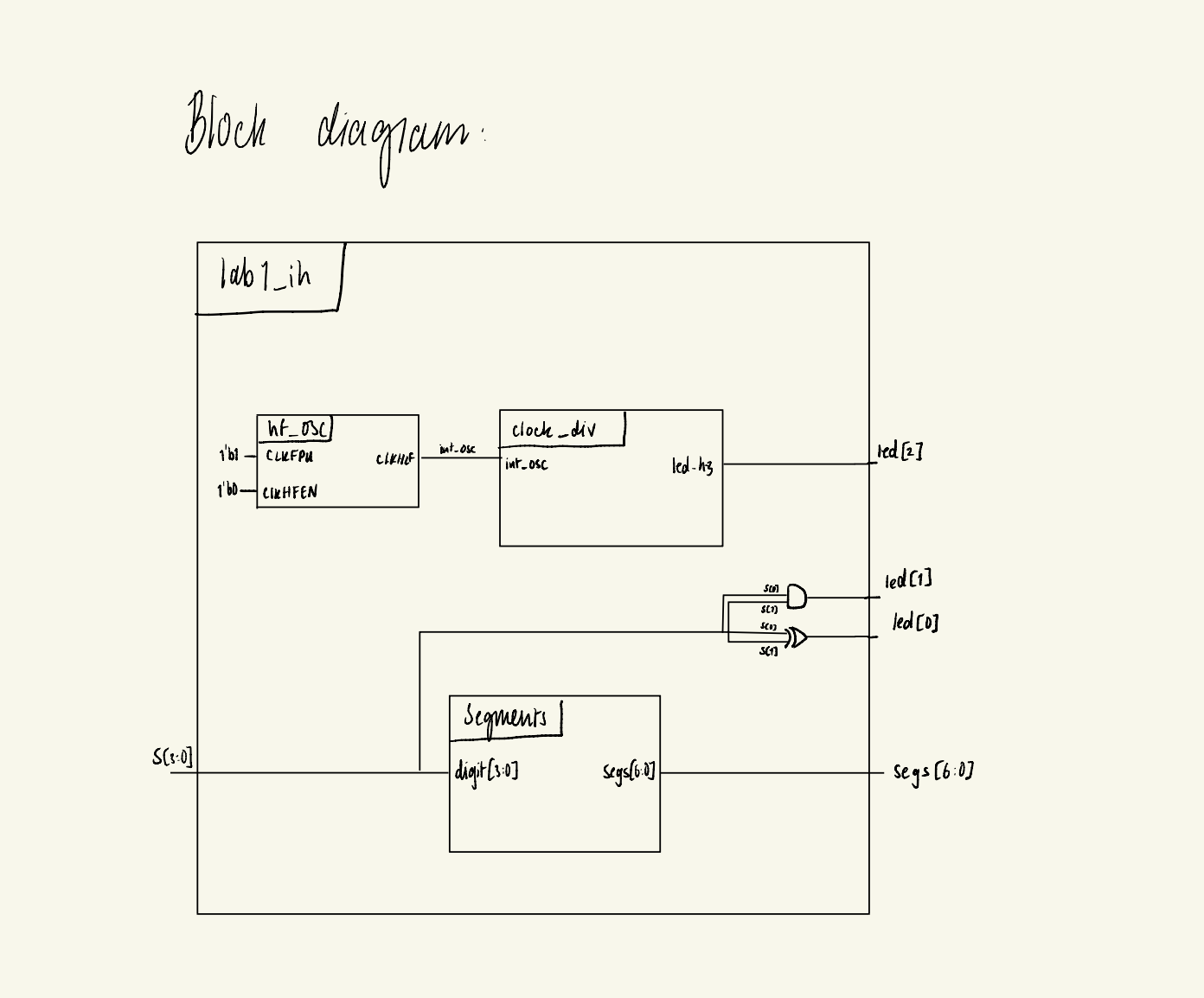
The top-level module, lab1_ih, accepts switch inputs s[3:0] and drives outputs led[2:0] and segs[6:0]. It instantiates three submodules: the high-speed oscillator (hf_osc), the seven-segment priority encoder (segments), and the 2.4 Hz clock divider (clock_div).
Schematic
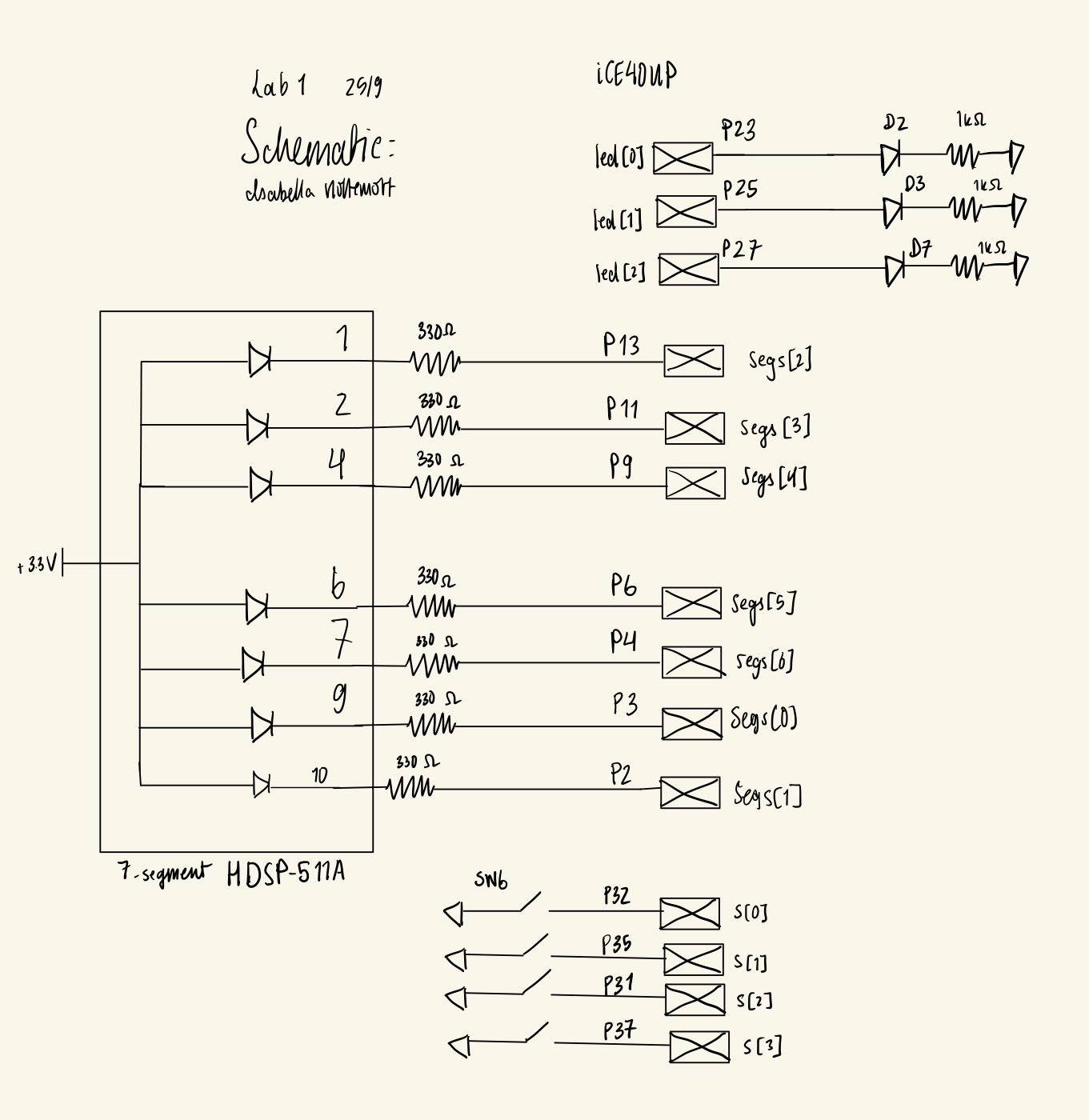
The schematic illustrates the breadboard wiring, including the 300 Ω series resistors used to limit current to both the seven-segment display and the on-board LEDs. Internal 100 kΩ pull-ups ensured that the active-low switch (SW7) did not float.
Results and Discussion
The design met all functional objectives. Switch inputs produced the correct LED and seven-segment display behavior, verified both experimentally and through simulation. Testbenches were developed for all modules, confirming correct logic.
Testbench Simulation

The lab1_ih testbench evaluated all combinations of switch inputs. Output waveforms for both the LEDs and the seven-segment display matched expected behavior. The HSOSC primitive was instantiated in simulation to validate clock-driven logic.
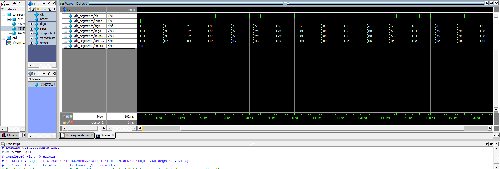
The segments module testbench confirmed correct encoding for all input combinations. Segment outputs matched the expected one-hot activations.
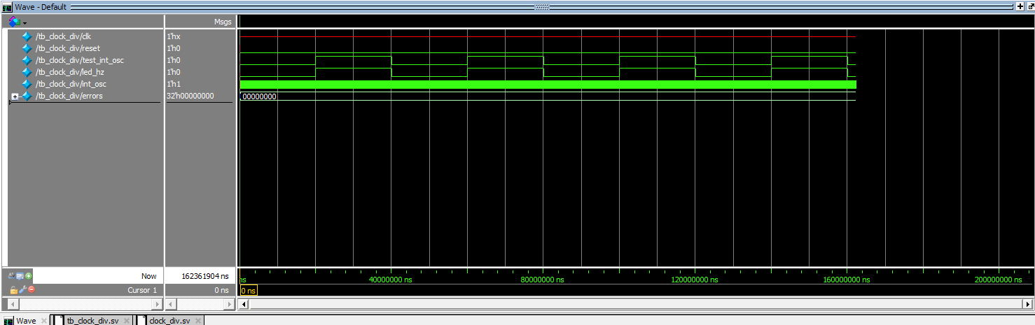
The clock_div testbench generated a model oscillator ticking every 20,000,000 simulation time units, corresponding to the intended 2.4 Hz blink frequency derived from a 48 MHz input clock. The divided clock output aligned precisely with the modeled reference.
Conclusion
This lab successfully demonstrated correct operation of the UPduino v3.1 FPGA and the E155 Development Board. The design verified the board’s assembly, confirmed the functionality of the on-board HSOSC, and produced correct LED and seven-segment display behavior.
AI Prototype Summary
The prompt that I provided the LLM was: “Write SystemVerilog HDL to leverage the internal high speed oscillator in the Lattice UP5K FPGA and blink an LED at 2 Hz. Take full advantage of SystemVerilog syntax, for example, using logic instead of wire and reg.”
The LLM’s response, as well as my evaluation of the response, can be found here